PHENIX 060
![]()
Logo by Chris Apers
|
The PHENIX 060 was designed from
March 98 to July 99. My routing was 100% manual with 4 layers and tooks 9 weeks. The mainboard prototype was assembled at August 99, the 4th & 5th and was debugged up to September 99, the 29th. I presented officially my PHENIX 060 at Hannover in November, the 19th & 20th during a computer show. In december 1999, the PHENIX 060 project was killed by the three developpers of the OS (Dolmen) that announced they will not finish this last one. The PHENIX is now defintively dead, after a birth in August 1999, the 11th, a coincidence, the day of a total eclipse of the sun in France. Here are the last hardware modifications I did between APRIL 99 and JUNE 99:
|
Evaluation for the first production of 100 Phenix : P60_Fab1.jpg (37KB) - P60_Fab2.jpg (51KB) - P60_Fab3.jpg (64KB)
Photos of the prototype debugging : P60_debug1.jpg (61KB) - P60_debug2.jpg (69KB)
Schematics of the AUDIO Circuit : P60_audio.jpg (29KB)
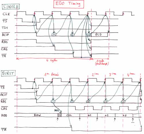
Chronograms of the EDO Ram accesses : P60_EDO.jpg (34KB)
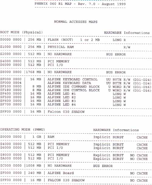
Memory Map : P60_MemMap.jpg (57KB)
Films of Phenix PCB layers : P60_PCB_Films.PDF (1,2MB)
Functionnal block diagram of the Alpine boards : P60_alpine.jpg (52KB)
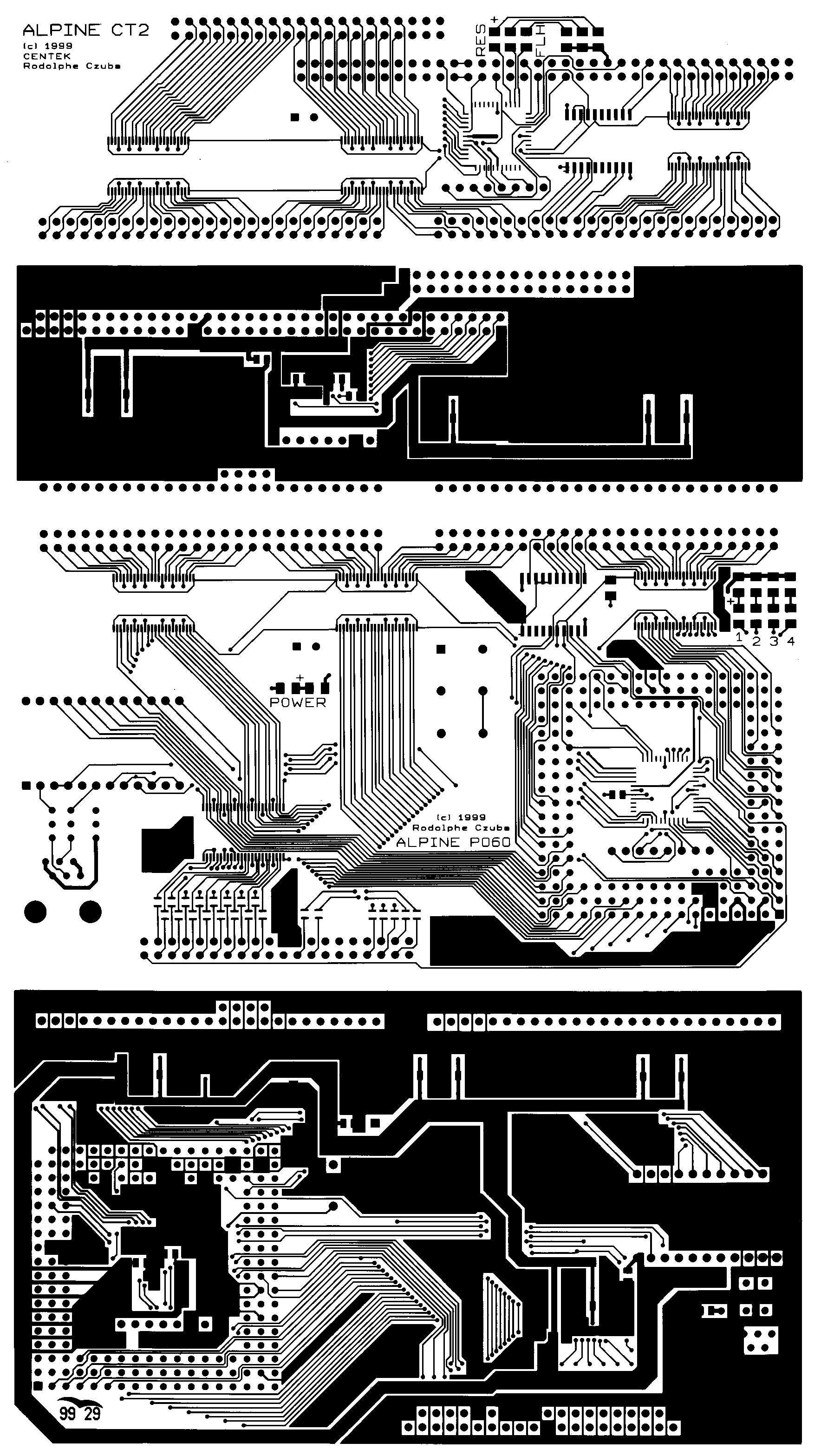
Layout of the ALPINE CT2 : Alpine_CT2.gif (10KB)
Layout of the ALPINE P60 : Alpine_P60.gif (21KB)
Films of Alpines PCB : Alpine_PCB_Films.gif (169KB)
Architecture Diagram

Features
| CPU | MOTOROLA MC68060 at 80 MHz expandable to TWO MC68060 at 80 MHz (240 MIPS). |
| BUS CPU | 060 32-Bit / 40 MHz (Half-speed mode). |
| BUS PHENIX | PCI 32-Bit / 33 MHz. |
| RAM | 2 SIMM sockets for up to 256 MBytes of 60ns EDO. BURST accesses (read/write) in 1 cycle at 40 MHz. |
| FLASH | 1
MBytes & 32-Bit width containing the BIOS
(SETUP/AUTOTEST/BOOT). Upgradable to 2 MBytes for embedded applications. |
| DSP | MOTOROLA
DSP56301 at 100 MHz (100 MIPS).
|
| USB |
|
| ULTRA-SCSI (USCSI) |
|
| VIDEO | PCI
S3 VIRGE DX with 4 MBytes of 35 ns EDO DRAM. Drivers for others models will be developed.
|
| AUDIO | ON-BOARD
Stereo 20-Bit circuit at 44.1 & 48 kHz with the
following on-board connectors :
|
| IDE (UDMA-33) |
|
| RTC | Timekeeping
+ 256 bytes module with NVRAM (Non Volatile Ram). Capability to suspend and wake up the PHENIX™. |
| INTERNAL SLOTS |
|
| KEYBOARD & MOUSE | Two PS/2 ports (Mini-Din 6). |
| CASE | Standard Mini ATX 2.1 Tower. |
| OPERATING SYSTEMS | DOLMEN
LINUX 060 |
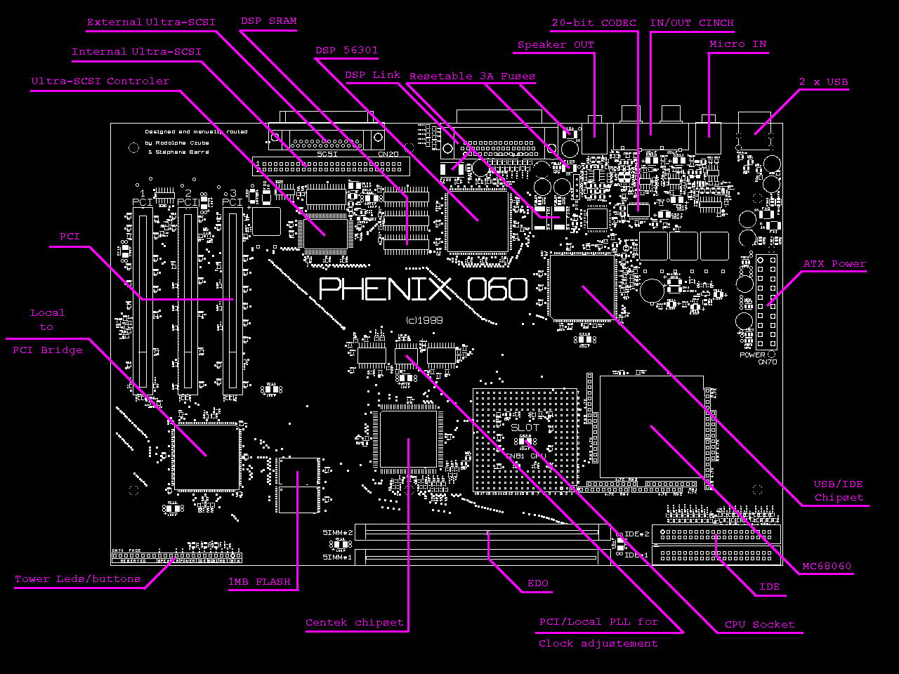
Implantation Diagram

